- 您现在的位置:买卖IC网 > Sheet目录480 > MTD2955VT4 (ON Semiconductor)MOSFET P-CH 60V 12A DPAK
�� �
�
�MTD2955V�
�POWER� MOSFET� SWITCHING�
�Switching� behavior� is� most� easily� modeled� and� predicted�
�by� recognizing� that� the� power� MOSFET� is� charge�
�controlled.� The� lengths� of� various� switching� intervals� (� D� t)�
�are� determined� by� how� fast� the� FET� input� capacitance� can�
�be� charged� by� current� from� the� generator.�
�The� published� capacitance� data� is� difficult� to� use� for�
�calculating� rise� and� fall� because� drain� ?� gate� capacitance�
�varies� greatly� with� applied� voltage.� Accordingly,� gate�
�charge� data� is� used.� In� most� cases,� a� satisfactory� estimate� of�
�average� input� current� (I� G(AV)� )� can� be� made� from� a�
�rudimentary� analysis� of� the� drive� circuit� so� that�
�t� =� Q/I� G(AV)�
�During� the� rise� and� fall� time� interval� when� switching� a�
�resistive� load,� V� GS� remains� virtually� constant� at� a� level�
�known� as� the� plateau� voltage,� V� SGP� .� Therefore,� rise� and� fall�
�times� may� be� approximated� by� the� following:�
�t� r� =� Q� 2� x� R� G� /(V� GG� ?� V� GSP� )�
�t� f� =� Q� 2� x� R� G� /V� GSP�
�where�
�V� GG� =� the� gate� drive� voltage,� which� varies� from� zero� to� V� GG�
�R� G� =� the� gate� drive� resistance�
�and� Q� 2� and� V� GSP� are� read� from� the� gate� charge� curve.�
�During� the� turn� ?� on� and� turn� ?� off� delay� times,� gate� current� is�
�not� constant.� The� simplest� calculation� uses� appropriate�
�values� from� the� capacitance� curves� in� a� standard� equation� for�
�voltage� change� in� an� RC� network.� The� equations� are:�
�t� d(on)� =� R� G� C� iss� In� [V� GG� /(V� GG� ?� V� GSP� )]�
�t� d(off)� =� R� G� C� iss� In� (V� GG� /V� GSP� )�
�The� capacitance� (C� iss� )� is� read� from� the� capacitance� curve� at�
�a� voltage� corresponding� to� the� off� ?� state� condition� when�
�calculating� t� d(on)� and� is� read� at� a� voltage� corresponding� to� the�
�on� ?� state� when� calculating� t� d(off)� .�
�At� high� switching� speeds,� parasitic� circuit� elements�
�complicate� the� analysis.� The� inductance� of� the� MOSFET�
�source� lead,� inside� the� package� and� in� the� circuit� wiring�
�which� is� common� to� both� the� drain� and� gate� current� paths,�
�produces� a� voltage� at� the� source� which� reduces� the� gate� drive�
�current.� The� voltage� is� determined� by� Ldi/dt,� but� since� di/dt�
�is� a� function� of� drain� current,� the� mathematical� solution� is�
�complex.� The� MOSFET� output� capacitance� also�
�complicates� the� mathematics.� And� finally,� MOSFETs� have�
�finite� internal� gate� resistance� which� effectively� adds� to� the�
�resistance� of� the� driving� source,� but� the� internal� resistance�
�is� difficult� to� measure� and,� consequently,� is� not� specified.�
�The� resistive� switching� time� variation� versus� gate�
�resistance� (Figure� 9)� shows� how� typical� switching�
�performance� is� affected� by� the� parasitic� circuit� elements.� If�
�the� parasitics� were� not� present,� the� slope� of� the� curves� would�
�maintain� a� value� of� unity� regardless� of� the� switching� speed.�
�The� circuit� used� to� obtain� the� data� is� constructed� to� minimize�
�common� inductance� in� the� drain� and� gate� circuit� loops� and�
�is� believed� readily� achievable� with� board� mounted�
�components.� Most� power� electronic� loads� are� inductive;� the�
�data� in� the� figure� is� taken� with� a� resistive� load,� which�
�approximates� an� optimally� snubbed� inductive� load.� Power�
�MOSFETs� may� be� safely� operated� into� an� inductive� load;�
�however,� snubbing� reduces� switching� losses.�
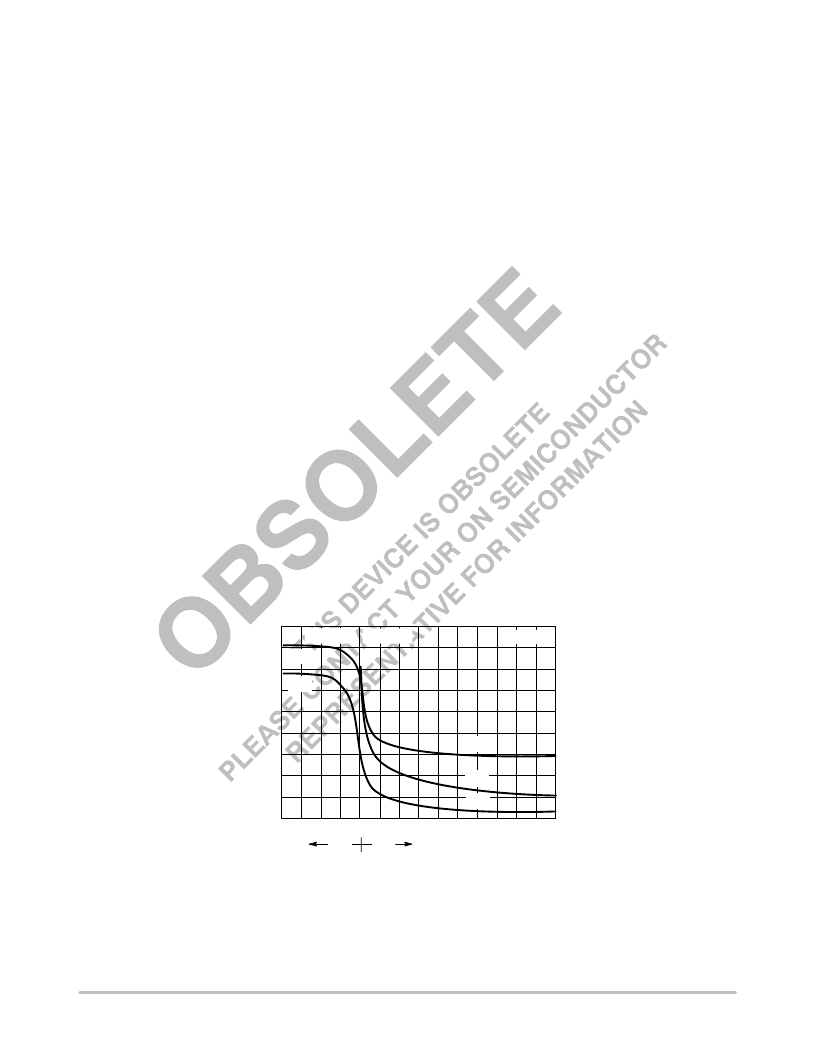
�1800�
�1600�
�C� iss�
�V� DS� =� 0� V�
�V� GS� =� 0� V�
�T� J� =� 25� °� C�
�1400�
�1200�
�1000�
�800�
�600�
�400�
�200�
�C� rss�
�C� iss�
�C� oss�
�C� rss�
�0�
�10�
�5�
�0�
�5�
�10�
�15�
�20�
�25�
�V� GS�
�V� DS�
�GATE?TO?SOURCE� OR� DRAIN?TO?SOURCE� VOLTAGE� (VOLTS)�
�Figure� 7.� Capacitance� Variation�
�http://onsemi.com�
�4�
�发布紧急采购,3分钟左右您将得到回复。
相关PDF资料
MTD3010N
PHOTO DIODE 900NM DOME CLR TO-18
MTD3010PM
PHOTO DIODE 900NM DOME CLR TO-18
MTD3055VL
MOSFET N-CH 60V 12A DPAK
MTD3055V
MOSFET N-CH 60V 12A DPAK
MTD5010N
PHOTO DIODE 850NM DOME CLR TO-18
MTD5010W
PHOTO DIODE 850NM FLAT CLR TO-18
MTD5052N
PHOTO DIODE 525NM B/G CLR TO-18
MTD5052W
PHOTO DIODE 525NM FLAT CLR TO-18
相关代理商/技术参数
MTD2955VT4G
制造商:ONSEMI 制造商全称:ON Semiconductor 功能描述:Power MOSFET 12A, 60V P-Channel DPAK
MTD2N20
制造商:MOTOROLA 制造商全称:Motorola, Inc 功能描述:POWER FIELD EFFECT TRANSISTOR N-CHANNEL ENHANCEMENT-MODE SILICON GATE
MTD2N40E
制造商:ON Semiconductor 功能描述:Trans MOSFET N-CH 400V 2A 制造商:Rochester Electronics LLC 功能描述:- Bulk
MTD2N40ET4
制造商:Rochester Electronics LLC 功能描述:- Bulk
MTD2N50
制造商:MOTOROLA 制造商全称:Motorola, Inc 功能描述:POWER FIELD EFFECT TRANSISTOR N-CHANNEL ENHANCEMENT-MODE SILICON GATE DPAK FOR SURFACE MOUNT OR INSERTION MOUNT
MTD2N50E
制造商:MOTOROLA 制造商全称:Motorola, Inc 功能描述:TMOS POWER FET 2.0 AMPERES 500 VOLTS RDS(on) = 3.6 OHM
MTD2N50E1
制造商:Rochester Electronics LLC 功能描述:- Bulk
MTD3010N
功能描述:PHOTO DIODE 900NM DOME CLR TO-18 RoHS:是 类别:传感器,转换器 >> 光学 - 光电检测器 - 光电二极管 系列:- 标准包装:1 系列:- 波长:850nm 颜色 - 增强型:- 光谱范围:400nm ~ 1100nm 二极管类型:引脚 nm 下响应率:0.62 A/W @ 850nm 响应时间:5ns 电压 - (Vr)(最大):50V 电流 - 暗(标准):1nA 有效面积:1mm² 视角:150° 工作温度:-40°C ~ 100°C 封装/外壳:径向,5mm 直径(T 1 3/4) 其它名称:475-2649-6